|
Pong on the C-One
Always use the latest version of Quartus, the free FPGA development tool by Altera. The version that has been used for this tutorial is Quartus II web edition V4.2. Download and install the program according to the instructions from Altera. Although the software is free, you need to obtain a license file, which is also free. The license file is sent to you via eMail. Copy the file to your Quartus program directory, and specify the path by choosing te menu item 'License setup' from the menu 'Tools'. Now you need a point to start from. To spare you the time to make a new project, enter all the pin names and numbers and implementing the graphics bus multiplexer, just get a snapshot from the project directory from this file. Make a new subdirectory in your Quartus design folder, and unpack the archive into that subfolder. Now open the project called 'a1k100' with the 'open project...' function from the File menu as shown in this picture: 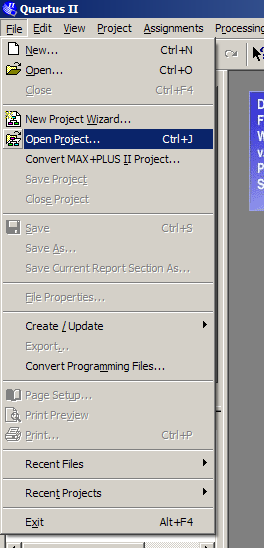
Now you see a lot of windows - we only need one, and that's the toplevel design file. The name is a1k100.bdf. You can either bring it to front by closing the other windows that are in the way, or by double-clicking the filename in the 'device design files' listing at the left of the screen. 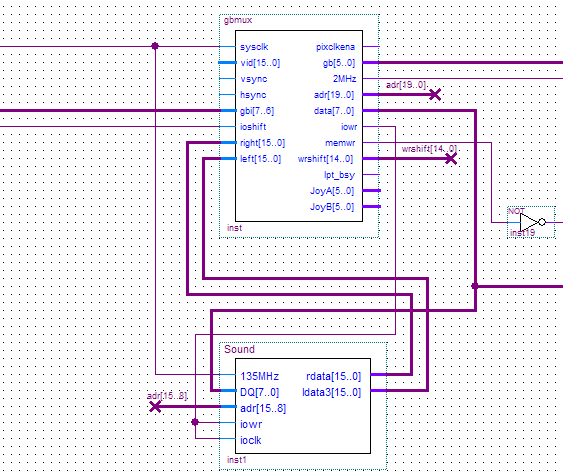
What you have opened here is the core that is automatically loaded into the 1k100 before you have chosen any core (starting with system flash V0.41 and higher). The design that you can see here is good for transferring roms into the S-ram of the CPU/RAM card, and it also contains parts of the CPC core, for example the AY8912 sound chip. This might be handy for you if you want to make a core that clones a computer with that same sound chip. You are free to use the source for any C-One core, but commercial use, or use on other platforms is prohibited. The above excerpt shows the toplevel design file. Think of it as the schematics of the design. You can double-click the blocks to enter the other design blocks. However, this is not needed for this tutorial. We want to add a design to the existing blocks. A very good and simple example is the Pong game from http://fpga4fun.com. Get the two design files pong.zip and hvsync_generator.zip. Unpack the two files into the project directory, and choose 'Add/Remove files in Project' from the Project directory: 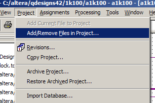
In the following requester, klick on the '...' button: 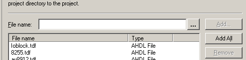
..and choose the two files that you have unpacked into the project directory: 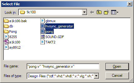
Confirm your choice with the 'open' button, then leave the menu with the 'OK' button. Now Quartus knows that the two Verilog design files are also part of the project, but before you can place them in the toplevel design file, you need to generate symbol blocks from the verilog files. A pre-processor checks what inputs and outputs the design file has, and automatically draws a symbol that you can place as many times as you need it in your design. We'll only need the Pong game once, but the 'place more than once' option comes handy if you're cloning a computer that has the same chip twice (for example port chips). To generate the symbols, you need to make the file that you want to generate the symbol of the 'current file'. This is simply done by double-clicking the file in the 'device design files' list at the left of the screen. Double-click the file 'pong.v'. Now choose the menu item 'Create symbol files for current file' from the File/Create/update menu: 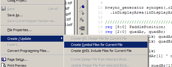
You should see this requester after a few seconds: 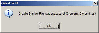
Confirm by clicking OK. You only need to create one symbol, because the two files are connected with each other on the source level. Quartus recognizes this automatically, and generates the graphical symbols for all files under the hirachy of the pong.v file. Now the symbols are ready to be used in the toplevel design file, that you should bring to the front by double-clicking the 'a1k100.bdf' file in the device design files listing at the left of the screen. Choose a place in the toplevel design file where you want to place the symbol - the bottom left is a good place for it. Right-click into the design file, and choose 'Symbol' from the 'Insert' menu: 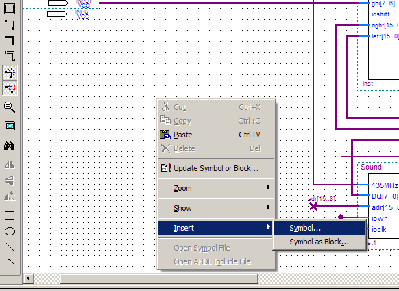
Now choose the Pong symbol from the project folder: 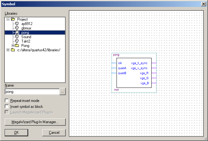
..and confirm by hitting the the OK button. A box has been attached to your mouse pointer that you can place in the graphical editor now. Drop the box by clicking the left mouse button about at this place: 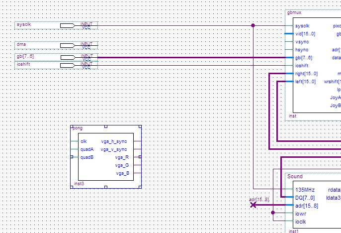
Now we need to wire up the Pong game inside the C-One enviroment. First, we need a clock. This is provided by the graphics bus multiplexer at the output 'pixclkena', and it runs at about 25 Mhz. Unfortunately, this clock has the wrong phase, but this is easily fixed with an inverter. Before we insert the inverter in the design, we're drawing a wire from the signal source to the place where the inverter will be placed. To do that, choose the 'thin wire' tool in the toolbar that is displayed at the left of the grapical editor: 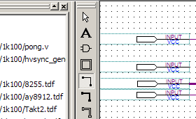
Now draw a wire like this - the routing does not have to be exactly the same: 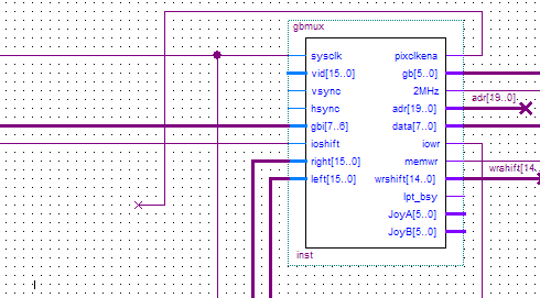
Now right-click the end of the wire, and choose 'Symbol' from the 'Insert' menu again. This time, choose the logic function 'not' from the Quartus libraries. The following two pictures show how to find the function: 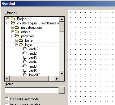
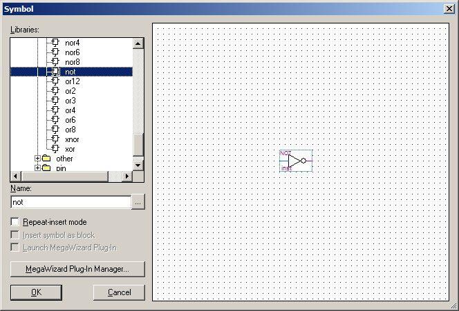
If you know the name of the function, you can also type it in the name field without clicking through the libraries path. Confirm your choice with the OK button, and place the inverter in the design, but not directly at the wire, because we don't want to connect it yet: 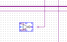
As you can see, the inverter has it's input on the wrong side, so before we connect it, we need to rotate or flip it. Right-click the symbol, and choose 'flip horizontal': 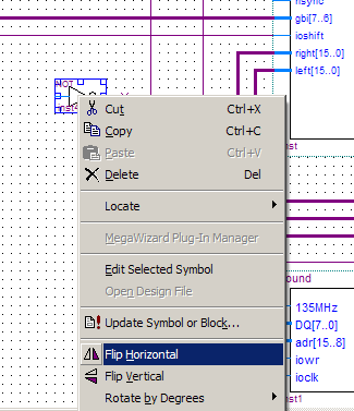
To make the first connection of the inverter, it must be moved to the end of the wire. Of course you still have the draw wire tool selected, and that is not good for moving parts around in the graphical editor, so choose the 'pointer' tool in the toolbar at the left of the graphical interface: 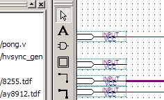
Now move the inverter with it's input to the open end of the wire by holding down the left mouse button while moving it. When the inverter is in place, just release the left mouse button, and the input is connected. Now choose the wire tool again, and make a connection between the output of the inverter, and the input of the pong game like this: 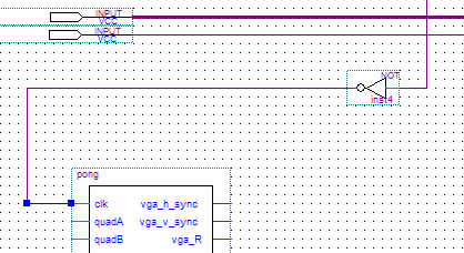
Now the sync lines need to be connected to the graphics bus multiplexer. At this point, we don't care if the outputs of the pong game are positive or negative syncs - the graphics bus multiplexer just passes on the signals directly to the monitor without looking at them (FYI: This Pong uses negative syncs). It's the responsibility of the core developer to generate the right syncronisation signals. However, most monitors accept both positive and negative syncs, so both should be fine. Connect the sync signals as shown in this picture: 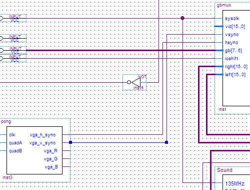
The RGB output of the Pong game is a bit tricky, because it's only one bit per colour component. The C-One has a lot more bits per colour component, and to reach the best brightness and contrast, we want to control all bits with Pong. This is done with the 'wire' logic function - connect wires to the RGB outputs like this: 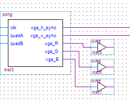
Now we need more than one wire on the other side of the buffer. This is done with the 'thick wire' tool - choose that tool by clicking on it in the toolbar like this: 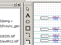
Of course, the kind of wire you're drawing with that tool is not just a 'thick wire'. It is a bundle of wires that can contain any number of signals. Using buses in a schematic design gives a lot more overview, because by just giving the right names to the buses, the signals are connected. A visible connection is not necessary, and would only confuse the viewer, as the following example shows. Draw the bus lines to the outputs of the buffers like this: 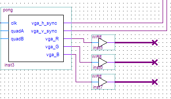
..and with the same tool, draw a bus line to the graphics bus multipleer like this: 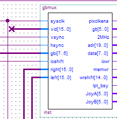
We're almost there! As mentioned before, the signals on bus lines are just connected by giving them the right names. This is done by switching back to the pointer tool, and clicking on the bus wires once. A blinking cursor appears that prompts you to enter signal names. Enter 'vid[15..0]' as signal name for the bus wire on the graphics bus multiplexer: 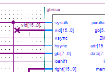
Next, give names to the three bus wires on the Pong output wires. You need to know which vid line has which function: The C-One uses five bits for red, six bits for green, and five bits for blue. They are assigned like this: red[4..0] are assigned to vid[4..0] green[5..0] are assigned to vid[10..5] blue[4..0] are assigned to vid[15..11] With this knowledge, you can name the bus wires on the Pong outputs like this: 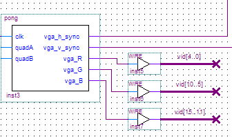
The last step of wiring up the pong game is the controls. Use the bus wire ('thick wire') tool to draw the joystick 'port A' bus and name it as explained above to have schematics like in this picture: 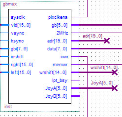
..and this brings the controls to the Pong core: The thin wires are also named with the pointer tool, just like the bus wires. The choice of lines is random at this point, because we don't have an Amiga or Atari ST mouse that has a quadrature output (at least not here in Magdeburg). Give us a few days for the final selection of lines. 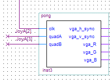
Now it's time to start the compile. Either choose 'Start Compile' from the 'Processing' menu, press CTRL-L, or click on the purple play button in the upper tool bar. You (and we!) are using a completely new version of Quartus, so some files need to be converted - just let Quartus convert everything to the new version. Depending on the speed of your computer, you should get this window after a few minutes: 
You can ignore the warnings - they are mostly due to unused inputs and outputs of subdesigns, and don't have an effect on the function of the generated core. Quartus has now generated the configuration stream for the 1k100 FPGA, and that's the file called a1k100.rbf: 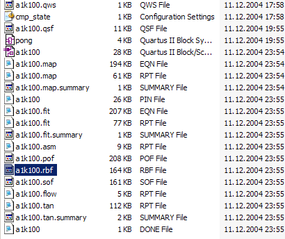
The suffix RBF stands for 'raw binary file', and it is the file type that BigBoot expects. Copy this file to a CF card and re-name it to '6fpga.bin' (or whatever number you want to give it). Further, we need a drive.bin file that tells the 1k30 FPGA what to do after the 1k100 has been configured. Just copy it from the C64 NTSC core, and rename it to 6drive.bin - it does exactly what we need: Switch the graphics multiplexer to the 1k100, and disconnect the 1k30 from the system address and data bus. To view the core by name in BigBoot, you need a text file that contains the name. Just use the Windows Notepad program to make a text file called '6desc.txt' with a single line in it. The result of the first chapter of this tutorial can be summarized with these two archives: The project directory after these worksteps and the resulting core that should be playable with an Amiga mouse (please report back!). A little bit of theory: The Pong core from http://fpga4fun.com generates a picture rate of about 64Hz, and a horizontal frequency of 33khz. The files as they come from Jean P. Nicolle's website need a little bit of tweaking to match the center of the monitor, and to have exact blanking periods. Some monitors won't display anything at all with the current settings. Proper tweaking and input device adaption is part of the next chapter. |